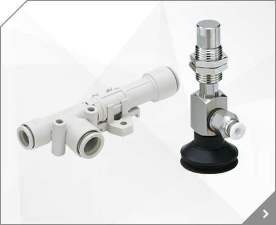
The ZP, ZP2 and ZP3 series lateral entry adapters offer a wide variety of cup diameters, materials and designs to suit multiple applications. The adapters are available with SMC's acclaimed built-in one-touch fittings. Buffer types are available with strokes up to 50mm, depending on the series. Lateral vacuum entry, With rotating or non-rotating buffer, Built-in one-touch fitting, Pad
The ZP, ZP2 and ZP3 series lateral entry adapters offer a wide variety of cup diameters, materials and designs to suit multiple applications. The adapters are available with SMC's acclaimed built-in one-touch fittings. Buffer types are available with strokes up to 50mm, depending on the series. Lateral vacuum entry, With rotating or non-rotating buffer, Built-in one-touch fitting, Pad
The ZPT series vacuum cups are available in diameters from 2 to 125mm, 6-cup materials, and 4-cup designs (flat, flat with ribs, deep and bellows), to suit multiple applications. Vertical vacuum entry connections can be made via one-touch fittings or threaded connections. Optional buffers can be ordered with up to 50mm stroke. SMC's ZP2 series vacuum pads are available in diameters from
The ZPT series vacuum cups are available in diameters from 2 to 125mm, 6-cup materials, and 4-cup designs (flat, flat with ribs, deep and bellows), to suit multiple applications. Vertical vacuum entry connections can be made via one-touch fittings or threaded connections. Optional buffers can be ordered with up to 50mm stroke. SMC's ZP2 series vacuum pads are available in diameters from
The ZPT series vacuum cups are available in diameters from 2 to 125mm, 6-cup materials, and 4-cup designs (flat, flat with ribs, deep and bellows), to suit multiple applications. Vertical vacuum entry connections can be made via one-touch fittings or threaded connections. Optional buffers can be ordered with up to 50mm stroke. SMC's ZP2 series vacuum pads are available in diameters from
The ZPT series vacuum cups are available in diameters from 2 to 125mm, 6-cup materials, and 4-cup designs (flat, flat with ribs, deep and bellows), to suit multiple applications. Vertical vacuum entry connections can be made via one-touch fittings or threaded connections. Optional buffers can be ordered with up to 50mm stroke. SMC's ZP2 series vacuum pads are available in diameters from
The ZPT series vacuum cups are available in diameters from 2 to 125mm, 6-cup materials, and 4-cup designs (flat, flat with ribs, deep and bellows), to suit multiple applications. Vertical vacuum entry connections can be made via one-touch fittings or threaded connections. Optional buffers can be ordered with up to 50mm stroke. SMC's ZP2 series vacuum pads are available in diameters from
The ZP, ZP2 and ZP3 series lateral entry adapters offer a wide variety of cup diameters, materials and designs to suit multiple applications. The adapters are available with SMC's acclaimed built-in one-touch fittings. Buffer types are available with strokes up to 50mm, depending on the series. Lateral vacuum entry, With rotating or non-rotating buffer, Built-in one-touch fitting, Pad
The ZP, ZP2 and ZP3 series lateral entry adapters offer a wide variety of cup diameters, materials and designs to suit multiple applications. The adapters are available with SMC's acclaimed built-in one-touch fittings. Buffer types are available with strokes up to 50mm, depending on the series. Lateral vacuum entry, With rotating or non-rotating buffer, Built-in one-touch fitting, Pad
The ZPT series vacuum cups are available in diameters from 2 to 125mm, 6-cup materials, and 4-cup designs (flat, flat with ribs, deep and bellows), to suit multiple applications. Vertical vacuum entry connections can be made via one-touch fittings or threaded connections. Optional buffers can be ordered with up to 50mm stroke. SMC's ZP2 series vacuum pads are available in diameters from
The ZPT series vacuum cups are available in diameters from 2 to 125mm, 6-cup materials, and 4-cup designs (flat, flat with ribs, deep and bellows), to suit multiple applications. Vertical vacuum entry connections can be made via one-touch fittings or threaded connections. Optional buffers can be ordered with up to 50mm stroke. SMC's ZP2 series vacuum pads are available in diameters from
The ZP, ZP2 and ZP3 series lateral entry adapters offer a wide variety of cup diameters, materials and designs to suit multiple applications. The adapters are available with SMC's acclaimed built-in one-touch fittings. Buffer types are available with strokes up to 50mm, depending on the series. Lateral vacuum entry, With rotating or non-rotating buffer, Built-in one-touch fitting, Pad
The ZP, ZP2 and ZP3 series lateral entry adapters offer a wide variety of cup diameters, materials and designs to suit multiple applications. The adapters are available with SMC's acclaimed built-in one-touch fittings. Buffer types are available with strokes up to 50mm, depending on the series. Lateral vacuum entry, With rotating or non-rotating buffer, Built-in one-touch fitting, Pad
The ZPT series vacuum cups are available in diameters from 2 to 125mm, 6-cup materials, and 4-cup designs (flat, flat with ribs, deep and bellows), to suit multiple applications. Vertical vacuum entry connections can be made via one-touch fittings or threaded connections. Optional buffers can be ordered with up to 50mm stroke. SMC's ZP2 series vacuum pads are available in diameters from
The ZPT series vacuum cups are available in diameters from 2 to 125mm, 6-cup materials, and 4-cup designs (flat, flat with ribs, deep and bellows), to suit multiple applications. Vertical vacuum entry connections can be made via one-touch fittings or threaded connections. Optional buffers can be ordered with up to 50mm stroke. SMC's ZP2 series vacuum pads are available in diameters from
The ZPT series vacuum cups are available in diameters from 2 to 125mm, 6-cup materials, and 4-cup designs (flat, flat with ribs, deep and bellows), to suit multiple applications. Vertical vacuum entry connections can be made via one-touch fittings or threaded connections. Optional buffers can be ordered with up to 50mm stroke. SMC's ZP2 series vacuum pads are available in diameters from
The ZP, ZP2 and ZP3 series lateral entry adapters offer a wide variety of cup diameters, materials and designs to suit multiple applications. The adapters are available with SMC's acclaimed built-in one-touch fittings. Buffer types are available with strokes up to 50mm, depending on the series. Lateral vacuum entry, With rotating or non-rotating buffer, Built-in one-touch fitting, Pad
The ZP, ZP2 and ZP3 series lateral entry adapters offer a wide variety of cup diameters, materials and designs to suit multiple applications. The adapters are available with SMC's acclaimed built-in one-touch fittings. Buffer types are available with strokes up to 50mm, depending on the series. Lateral vacuum entry, With rotating or non-rotating buffer, Built-in one-touch fitting, Pad
The ZPT series vacuum cups are available in diameters from 2 to 125mm, 6-cup materials, and 4-cup designs (flat, flat with ribs, deep and bellows), to suit multiple applications. Vertical vacuum entry connections can be made via one-touch fittings or threaded connections. Optional buffers can be ordered with up to 50mm stroke. SMC's ZP2 series vacuum pads are available in diameters from
SMC's series ZP, ZP2 and ZP3 vacuum pads offer a complete line of pad options to meet all of your handling and transfer needs. A wide range of sizes, shapes and materials allow design engineers the flexibility to choose the appropriate pad configuration, making the ZP, ZP2, and ZP3 suitable for a variety of routine and unusual lifting applications.Heavy duty vacuum pad, Replacement part
